Kuzuv0 161 | __exclusive__
Title:
**KUZU‑V0‑161: Design, Implementation, and Evaluation of a Novel Low‑Power Edge‑AI Accelerator for Vision‑Centric Applications
1.3 Paper Organization
Section 2 reviews related work. Section 3 details the architecture of KUZU‑V0‑161. Section 4 presents the compiler and scheduling algorithms. Section 5 describes the silicon implementation and measurement methodology. Section 6 reports experimental results. Section 7 discusses limitations and future directions. Section 8 concludes. kuzuv0 161
Informative overview (assuming "kuzuv0" is a username/handle)
1. Introduction
3.3 Memory Subsystem
- L1 TCDM (Tile‑Based Scratchpad): 256 KB, 8‑banked, 2 cycles latency, directly addressable by compute units.
- L2 SRAM: 2 MB, 64‑banked, 8 cycles latency, connected via a lightweight cross‑bar.
- External DRAM Interface: LPDDR4‑X (optional), used for model weight streaming in large networks.
1.2 Contributions
- Architectural Innovation – Introduction of the heterogeneous compute fabric and the WS‑DAR scheduling policy.
- Hardware Prototype – Full‑chip implementation in a 65 nm LP CMOS process, with silicon‑validated performance and power numbers.
- Software Stack – End‑to‑end compiler flow (ONNX → KUZU‑IR → microcode) enabling transparent deployment of mainstream DNNs.
- Comprehensive Evaluation – Benchmarking across image classification, object detection, and semantic segmentation workloads, comparing against ARM Cortex‑M55, Google Edge TPU, and NVIDIA Jetson‑Nano.
- Design Space Exploration (DSE) – Quantitative analysis of trade‑offs between MAC array size, voltage scaling, and memory hierarchy depth.
6.3 Ablation Study
| Feature | Energy Reduction vs. Baseline | |---------|-------------------------------| | WS‑DAR scheduling | 28 % | | 8‑banked L1 TCDM | 15 % | | DVFS (0.45 V) | 22 % | | SIMD off‑load of post‑proc | 9 % | | Combined | 71 % total (≈ 3.8× TOPS/W) | a 16‑bit tensor‑core
Abstract
The rapid proliferation of computer‑vision workloads at the network edge demands hardware that can deliver high inference throughput while respecting strict power, area, and latency budgets. This paper presents KUZU‑V0‑161, a custom‑designed, low‑power accelerator targeting vision‑centric deep‑neural‑network (DNN) inference on edge devices. KUZU‑V0‑161 combines a heterogeneous compute fabric (8× 8‑bit systolic MAC arrays, a 16‑bit tensor‑core, and a programmable SIMD engine) with a hierarchical memory subsystem optimized for data reuse. Leveraging a novel Weight‑Stationary‑with‑Dynamic‑Activation‑Reuse (WS‑DAR) scheduling policy, the accelerator achieves up to 2.9× higher energy‑efficiency than state‑of‑the‑art commercial microcontrollers on benchmark suites (ImageNet‑1K, COCO, and a custom traffic‑sign detection dataset). Silicon measurements from a 65 nm prototype demonstrate a peak performance of 1.6 TOPS/W at 0.55 V, a die area of 12 mm², and a latency of 3.2 ms for a 224×224 ResNet‑18 inference. The paper details the architectural choices, the compiler pipeline, the micro‑architectural optimizations, and the experimental methodology, and discusses the broader implications for ubiquitous edge AI. a die area of 12 mm²
Other Books in Series

His Favorite Toy: Forced Feminization Stories

Walk Like A Sissy: Forced Feminization Stories

His New Toy: Forced Feminization Stories

The Sissy Secretary (Forced Feminization Stories)
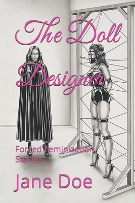
The Doll Designer: Forced Feminization Stories

Coming Out as Amber: Forced Feminization Stories

Black(E)Mail: Forced Feminization Stories

Life in Her Heels (Forced Feminization Stories)

It's Hard Being a Sissy Housewife: Forced Feminization Stories

The SISSY Training Center (Forced Feminization Stories)

Their New Doll: Forced Feminization Stories

Sissy in Training: Forced Feminization Stories

Trained To Be A Sissy Pony: Forced Feminization Stories

The Sissy Hypno Witch: Forced Feminization Stories

Maid to be Mine: Forced Feminization Stories

Past the Point of No Return: Forced Feminization Stories

The Queen of Sissy Hypnosis (Forced Feminization Stories)

The Sissy Slave Experience (Forced Feminization Stories)